Doc no. SK-404DatasheetRev 2026.11Sheet 2.3 of 4
Heater Driver v4
12 V / 100 W through-hole PCB heater driver that latches off on over-current and over-temperature.
Prototype
Source on GitHub
$ ./scripts/run_all.sh
Block diagram
Characteristics
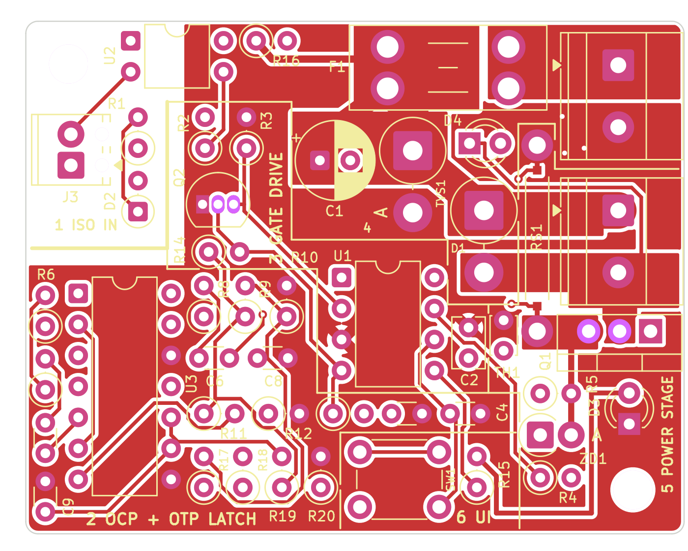
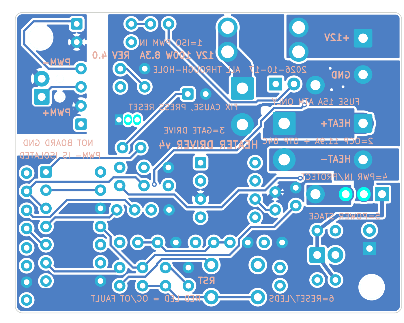
| Rating | 12 V, 100 W (8.33 A) into a heater load; 2-layer board, 54 × 42 mm, 100 % through-hole |
|---|---|
| Switch | IRFB7430 MOSFET at 1.3 mΩ: about 0.09 W dissipated at full load |
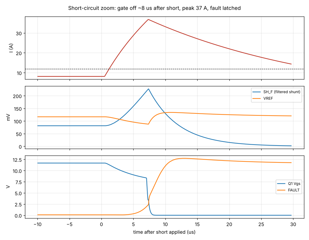
| Over-current | Latching trip at 11.9 A; in simulation the gate is off about 7 µs after a short, with a peak of about 37 A |
| Over-temperature | NTC thermistor next to the shunt and MOSFET latches the board off at about 84 °C (83.8 °C simulated) |
| Backup | 15 A ATM fuse, and a TVS that clamps supply spikes at 25 V |
| Verification | ngspice virtual test, ERC and DRC reports, an IPC-2221 copper current check and a 24-step bring-up checklist |
Overview & build notes
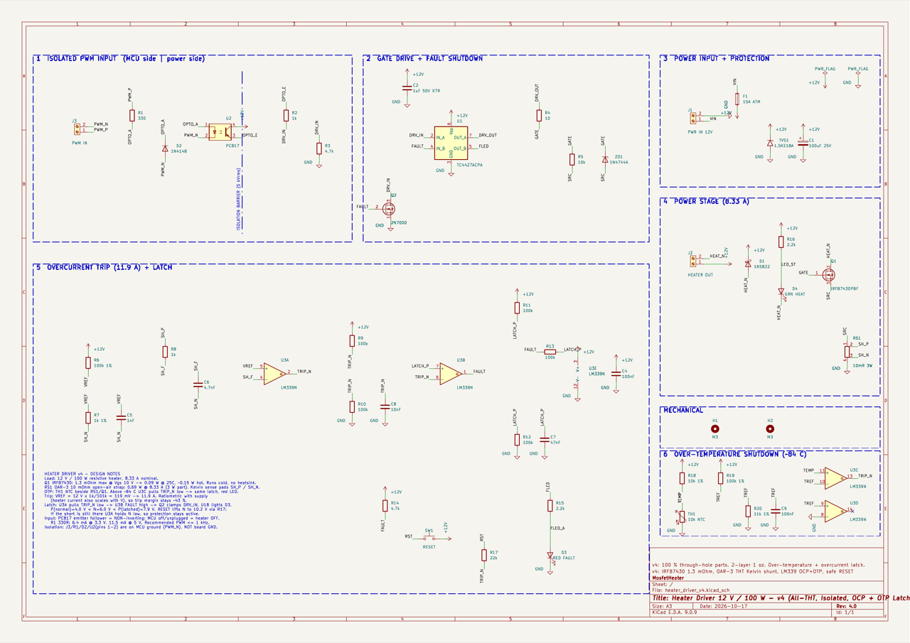
A 12 V supply feeds the board at J1, and a resistive heater up to 100 W (8.33 A) connects to J2. An isolated 3.3–5 V PWM signal (up to 1 kHz) drives J3 through a PC817 optocoupler and TC4427A gate driver, switching the low-side IRFB7430 MOSFET while staying completely OFF if the microcontroller is unplugged.
Revision 4 replaces all remaining SMD passives from v3 so the board is 100 % through-hole and can be soldered with an ordinary iron following a numbered bottom-up order. An open-air 3 W OAR3 shunt stands off the PCB with Kelvin sense pads, and an NTC thermistor beside the shunt and MOSFET shares an LM339 latching shutdown loop that lights the red FAULT LED until RESET is pressed.
Because high-current faults arc before a fuse melts, over-current protection trips in simulation at 11.9 A (~7 µs gate turn-off), backed up by a 15 A ATM mini blade fuse and a 1.5KE18A TVS diode across the input rail.
Figures & renders
Files & artifacts
| Kind | File | Details | Size |
|---|---|---|---|
| Gerber | heater_driver_v4_GERBERS_for_fab.zip | Ready-to-upload 2-layer fabrication archive (54 × 42 mm, 1.6 mm FR-4) | 148 KB |
| Guide | heater_driver_v4_placement_guide.pdf | Board map, solder order, X/Y table and 46 per-part placement cards | 1.2 MB |
| Checklist | heater_driver_v4_test_checklist.pdf | 24-step unpowered, no-load, gate-drive, load soak and trip verification protocol | 87 KB |
| BOM | heater_driver_v4_BOM.csv | All 46 through-hole components with values, packages and manufacturer part numbers | 5 KB |
| KiCad | heater_driver_v4.kicad_pcb | Routed 2-layer board source on GitHub | GitHub |
| KiCad | heater_driver_v4.kicad_sch | Full schematic source on GitHub | GitHub |